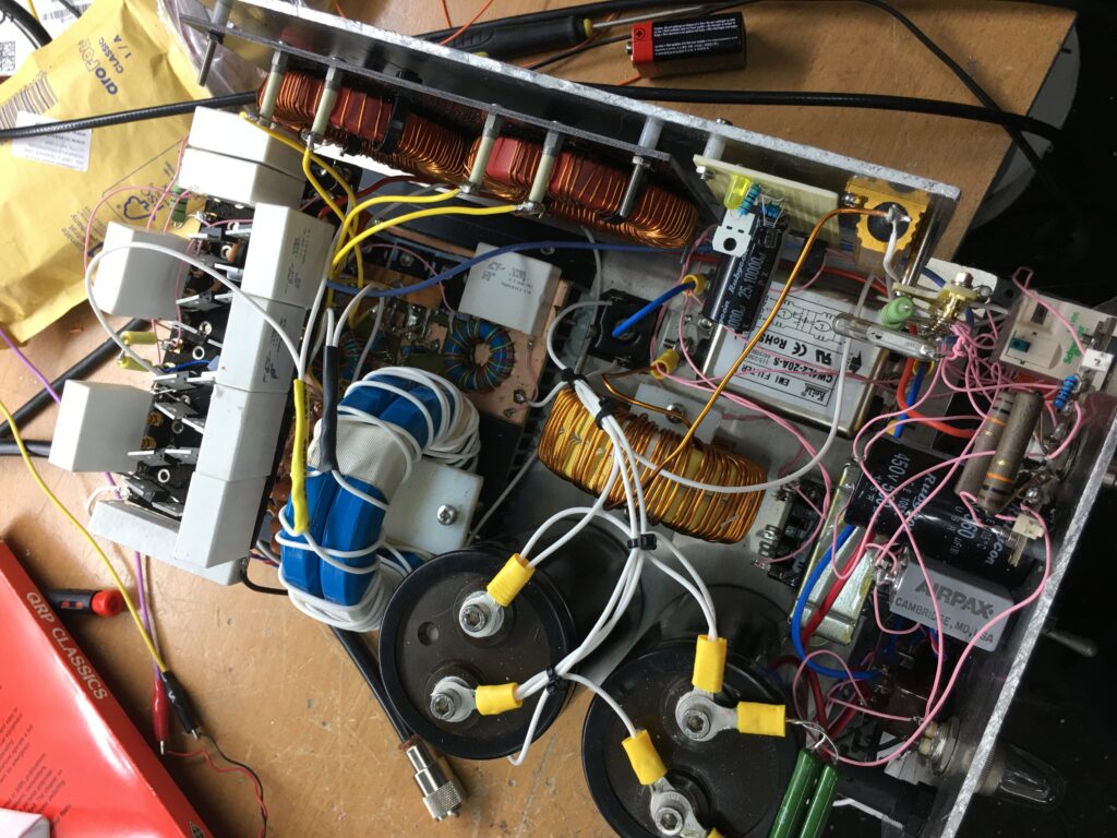
If you want to build a big vacuum tube RF amplifier you invariably need a high voltage power supply for the anodes of the power valves. Traditionally this has meant big transformers with large filter chokes and capacitors. These power supplies often weigh a ton and take up valuable space in the shack.
My friend Paul Bennett (G7RHT) came up with this interesting design to try and provide a high voltage SMPS that would not only be able to provide the volts but also the amps at a fraction of the weight and size of a traditional psu.
This is Paul’s description of how it works…
Theory of operation
“The circuit uses a UCC25600 resonant controller IC driving a full bridge. The bridge connects to the load via a resonant circuit, isolating/matching transformer and 8 stage voltage multiplier. The resonant circuit and transformer turns ratio are chosen to match the required power to the multiplier, drawing an approximate sinusoidal current. Maximum power occurs at minimum frequency slightly above resonance. The load current is lagging slightly so the transistors switch at a middling current, lower than the maximum but critically not zero. This helps the transistor capacitances switch and achieve “soft switching” with some additional capacitance across them. When the transistors turn off the voltage rise across them is delayed by the capacitor so they fully turn off before significant voltage has risen, this then reduces turn off switching loss. The lag of the load current then swings the voltage until the diode of the opposite FET in the bridge leg catches it and starts to conduct. When this FET turns on the voltage across it is already next to zero so there are no turn on losses.
As the frequency increases the current becomes more inductive, becomes more triangular and lower amplitude, and the output reduces. The multiplier diode capacitances and recovery charges are absorbed into the resonance capacitance.
The transformer output was chosen to be around 400V pk which results in 800V pk across the multiplier diodes and 800V across the multiplier capacitors. The output is then around 8 x 400 = 3.2KV adjusted slightly up for the 14 x 240 = 3360V lamp test load. Stored energy approx 5J.
The chip doesn’t have a traditional reference and error amplifier like old school pwm chips, the frequency is controlled by current drawn from pin 2 intended to connect to the transistor of an opto coupler. So I used an external LM324 op amp. The set point is 0 to 5V on a pot derived from a precision 10.0V reference IC AD581. The LM324 error amplifier then compares this to the divided down output and drives the UCC25600 via some resistors to control the amount of frequency pull. The chip has an over current input which I don’t use. Under short circuit conditions there is no resonance just the inductor and the current remains sensibly controlled and triangular even with the control loop taking the frequency to minimum. Output voltage is adjustable down to approx 10% of maximum output, limited by the maximum frequency of around 250KHz.
Variable frequency rather duty cycle control makes the gate drive easy as these are just slightly less than 1:1 square waves. Dead time when no transistors are on allows time for the switching to occur. Two gate transformers are used, each driving diagonally opposite transistors. These have a 1:1:1 ratio so each FET is driven with slightly more than half the 15V control supply voltage.
The power supply can be keyed using the soft start input to the IC. If this is grounded the IC is shut off and switching stops. When released the frequency starts high at minimum power ramping down under control of the 0.1uF capacitor. When the output reaches the desired level the control loop catches and takes over frequency control.
AC input
The mains input is filtered, fused then feed to a soft charge circuit. The mains is rectified by a bridge and smoothed by two 2200uF 400V electrolytics. These are initially charged via a 50 ohm 50W resistor, then the resistor is shorted out by relay RL2. RL2’s coil is 110V DC which is powered across a 470uF capacitor charged via a half wave rectifier circuit and resistor. This then delays the relay closing giving time for the main electrolytics to charge. RL1’s coil is 240V AC across the mains and a normally closed contact resets the timing action when AC power is removed. Further contacts on both relays inhibit the control chip using the soft start input also used for keying.
A capacitive input filter has a poor power factor just drawing current at the peak of the mains. This is softened by the 1mH series inductor. A capacitive input filter on a traditional line frequency transformer would also have a poor power factor softened only by the transformer’s leakage inductance, so the 1mH replicates this.
Low power control DC supply is provided by a 240 to 18V 6VA transformer. The raw rectified output from this is approx 24V used for the fan. An LM340T15 linear regulator regulates the 15V.”
I built my own version of Paul’s design which has an output of 1500v although I have not found anything to use it with yet!!